Processador [ARM] Samsung Exynos para Laptops

Nemesis11

Power Member

Samsung to jump into laptop processor market with Exynos chip in H2​


With the global laptop computer market growing rapidly in the pandemic-caused work-and-learn from home era, Samsung Electronics Co. is working on a laptop version of its flagship mobile application processor (AP) chip Exynos.

According to industry sources on May 9, the South Korean tech giant will unveil a premium Exynos chip that can be used in laptops as well as smartphones in the second half of this year.

If the product hits the market, Samsung would become the first modern Windows laptop manufacturer to launch its own processor that works as the brain in its machines.
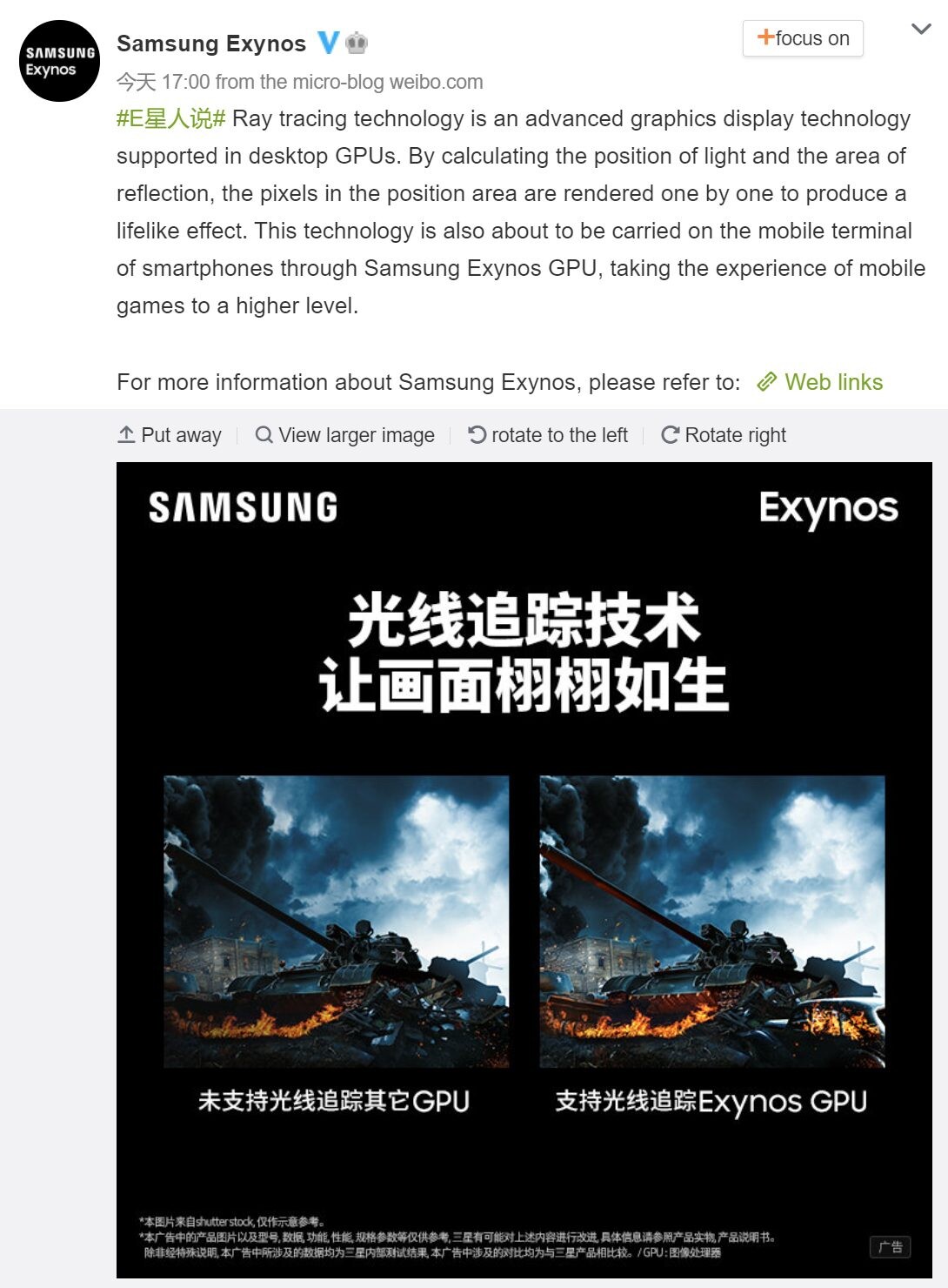
The new Exynos chip for laptops will use the graphics processing unit (GPU) jointly developed with US semiconductor company Advanced Micro Devices Inc. (AMD) to offer improved graphical technology, according to the sources.

“The new Exynos will offer improved functions, including extraordinary computing power and battery efficiency, by utilizing a 5-nanometer processing technology. It’s good for both laptops and smartphones,” said an industry source.
JUMP ON BANDWAGON

As the sales of PCs and laptops grow at a fast pace, global tech companies that have focused on smartphone AP chips are also unveiling chipsets for laptops to take on market leader Intel Corp., and Samsung is jumping on the bandwagon.

In November 2020, Apple Inc. launched the M1 chip, a desktop- and laptop-grade systems-on-chip (SoC) based on a British processor architecture known as ARM.
https://www.kedglobal.com/newsView/ked202105090002
 

RUMOR

Samsung reportedly already negotiating contract with AMD for mRDNA successor​


the throttling is stronger than expected, so after the first test, the performance drops by about 20%, and after the second test, the performance drops by about 30%. The important thing is that this 30% performance drop is higher than that of ARM’s latest Mali series. Even next year’s next-generation Mali lineup is slightly lower than the high-end peak performance…

It is worthwhile for Samsung to give up its own GPU and adopt AMD architecture. It is said that Samsung has gained confidence in this and is also negotiating a contract for the AMD mRDNA successor architecture. […]

(machine translation from Korean)
https://videocardz.com/newz/samsung...tiating-contract-with-amd-for-mrdna-successor
 

Samsung Exynos 2200 “Palmir” to feature AMD RDNA2 GPU codenamed “Voyager”​

The Exynos 2200 SoC would likely use Samsung 4LPP (4nm Low Power Plus node), however, the details on this node are still limited.
Ice Universe has shared two codenames related to this SoC. The processor itself is codenamed “Palimir” whereas the graphics subsystem supplied by AMD is codenamed “Voyager”, the leak revealed.

A fruit of Samsung and AMD collaboration is to debut early next year. It is rumored to feature ARM Cortex X2 core architecture, following the path of Exynos 2100 which ditched custom cores for ARM design.
https://videocardz.com/newz/samsung-exynos-2200-palmir-to-feature-amd-rdna2-gpu-codenamed-voyager

Baseado no rumor de um post de um user chinês(?)

AMD-Voyager-RDNA-GPU-768x203.png
 
Verdade seja dita, é mais que suficiente para um aparelho móvel. Duvido que haja muita gente a utilizar a capacidade do CPU de um 888 ou de um iPhone moderno. Nem há muitos cenários onde faça falta mais. Não andamos propriamente a fazer rendering em telemóveis.

O que interessa é a parte gráfica.
 
A questão é que, alegadamente, a Samsung tem pretensões de ter processadores próprios em Laptops.
O M1 da Apple deve ter feito disparar os alarmes em algumas empresas. Pelo menos até agora, Samsung e Google.

A performance naquele teste não é nada de especial, especialmente tendo em conta que usa o Cortex-X2. Dito isto, especula-se que aqueles 2.6 Ghz não sejam os Clocks finais.
 
Tem?
Mas eles não tinham abandonado e dispensado a equipa que desenvolvia os Mongoose?

Sei que há uns meses voltaram os rumores, mas que supostamente estariam a contratar para voltar a formar uma equipe, portanto na melhor das hipóteses só daqui a uma ano.
 
A Samsung não precisa de criar Custom Cores para ter pretensões em entrar no mercado Laptop. O X2, que deve estar a ser usado no CPU naquele Bench, é um Core criado pela ARM.
 
Quando falaste em processadores próprios assumi que estavas a falar de custom cores 😉

Tinha ideia que tinham fechado o centro em Austin, apesar de terem supostamente 2 cores em "desenvolvimento".

Neste caso o "trabalho" seria montar um SoC, basicamente integrando os componentes.
 
Sim deve ser isso dado ele apenas ter referenciado um core como X2, se bem que a mim isso me faz um pouco de confusão, parecem-me demasiados cores...
 
Já agora, o Android já terá versão ARMv9?
Ainda não e deve vir apenas com Android 13 no próximo ano.

No entanto código ARMv8 deverá correr em ARMv9 com alguns tweaks do kernel. Não irá tirar todo o proveito da nova ISA mas alguns ganhos da nova arquitectura são transparentes para o front-end.
 
E um outro rumor - a "tree" do kernel para os Exynos era a mesma do novo SoC do Google Pixel 6 - confirmado

What's inside the Google Pixel 6 Pro Teardown?​

blog-image-Google-Tensor-Application-Processor-3.jpg

The Tensor die has a die size (seal) of 10.38mm x 10.43mm = 108.26mm2. The following images show die marks and the die photo.
blog-image-Google-Tensor-Application-Processor-2.jpg

The die mark “S5P9845” conforms to the traditional Samsung Exynos processor naming rule,
We have heard of possible ties between the Google Tensor and Samsung Exynos processors, and our analysis of the Tensor die continues. It does appear that the foundry supplier for the Tensor die is Samsung. We will confirm the process node soon, which we expect is in Samsung’s 5LPE.
https://www.techinsights.com/blog/teardown/google-pixel-6-pro-teardown


Google's Tensor inside of Pixel 6, Pixel 6 Pro: A Look into Performance & Efficiency

On the silicon side, the chip has another model number, with the SoC’s fused chip identification following Samsung’s Exynos naming scheme. Here we find the chip has an ID of “0x09845000”, which corresponds to what would be S5E9845 (Edit: It's actually S5P9845). The latest Samsung LSI SoC, for reference, is the Exynos 2100, which is identified as the S5E9840.

Of course, why would the Google SoC follow an Exynos internal naming scheme? That’s where we can begin to see some of the provenance of the design. It’s been widely reported for some time that a few years back, Samsung opened up itself to semi-custom silicon design offers.
Screenshot-2021-11-08-at-17-37-56-Google-s-Tensor-inside-of-Pixel-6-Pixel-6-Pro-A-Look-into-Perform.png

https://www.anandtech.com/show/17032/tensor-soc-performance-efficiency

Será que esta pareceria se vai estender para lá dos smartphones? Será que irá incluir o IP GPU da AMD?
 
Back
Topo