THREAD de DIÁRIO DE BOSTO -> https://forum.zwame.pt/threads/amd-rdna-3-radeon-rx-7000-diario-de-bordo.1077211/
AMD RDNA 3 GPU Architecture Deep Dive: The Ryzen Moment for GPUs


https://www.tomshardware.com/news/amd-rdna-3-gpu-architecture-deep-dive-the-ryzen-moment-for-gpus
"RDNA3" Instruction Set Architecture
https://developer.amd.com/wp-content/resources/RDNA3_Shader_ISA_December2022.pdf
AMD RDNA 3 GPU Architecture Deep Dive: The Ryzen Moment for GPUs
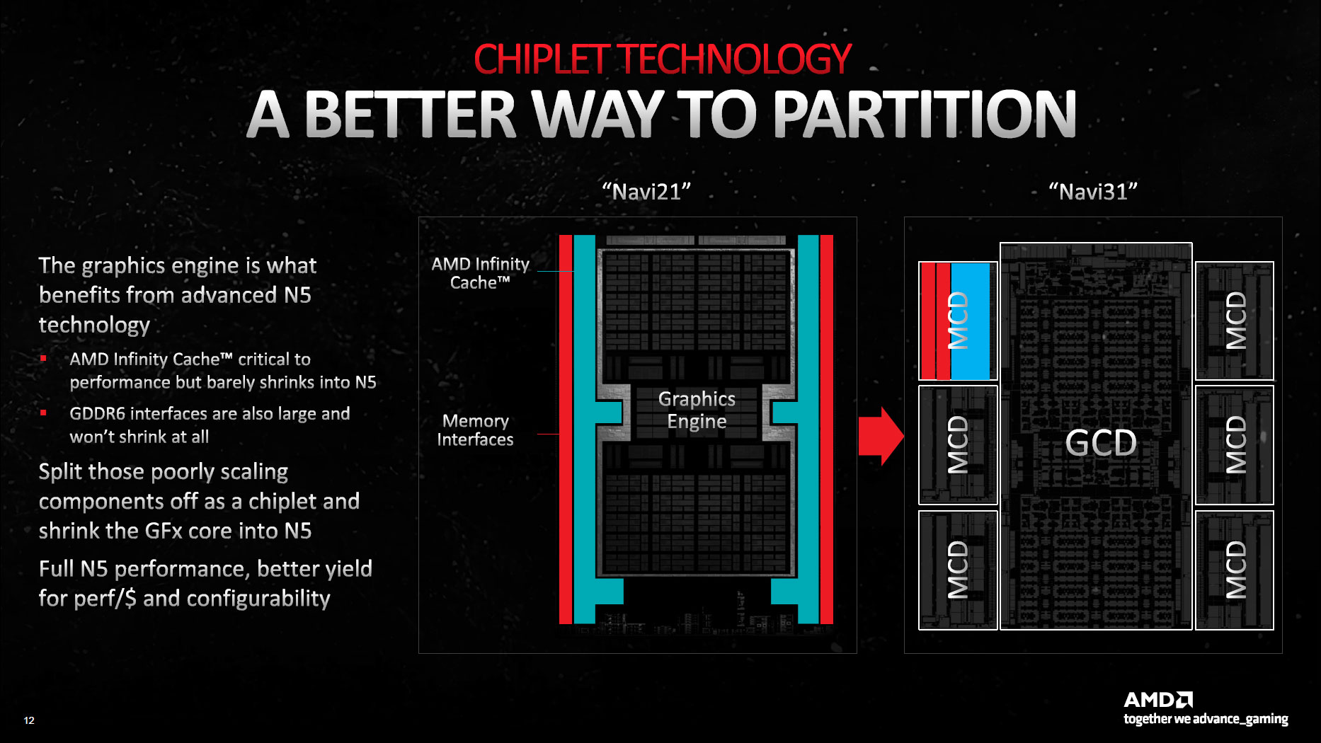
RDNA 3 and GPU Chiplets
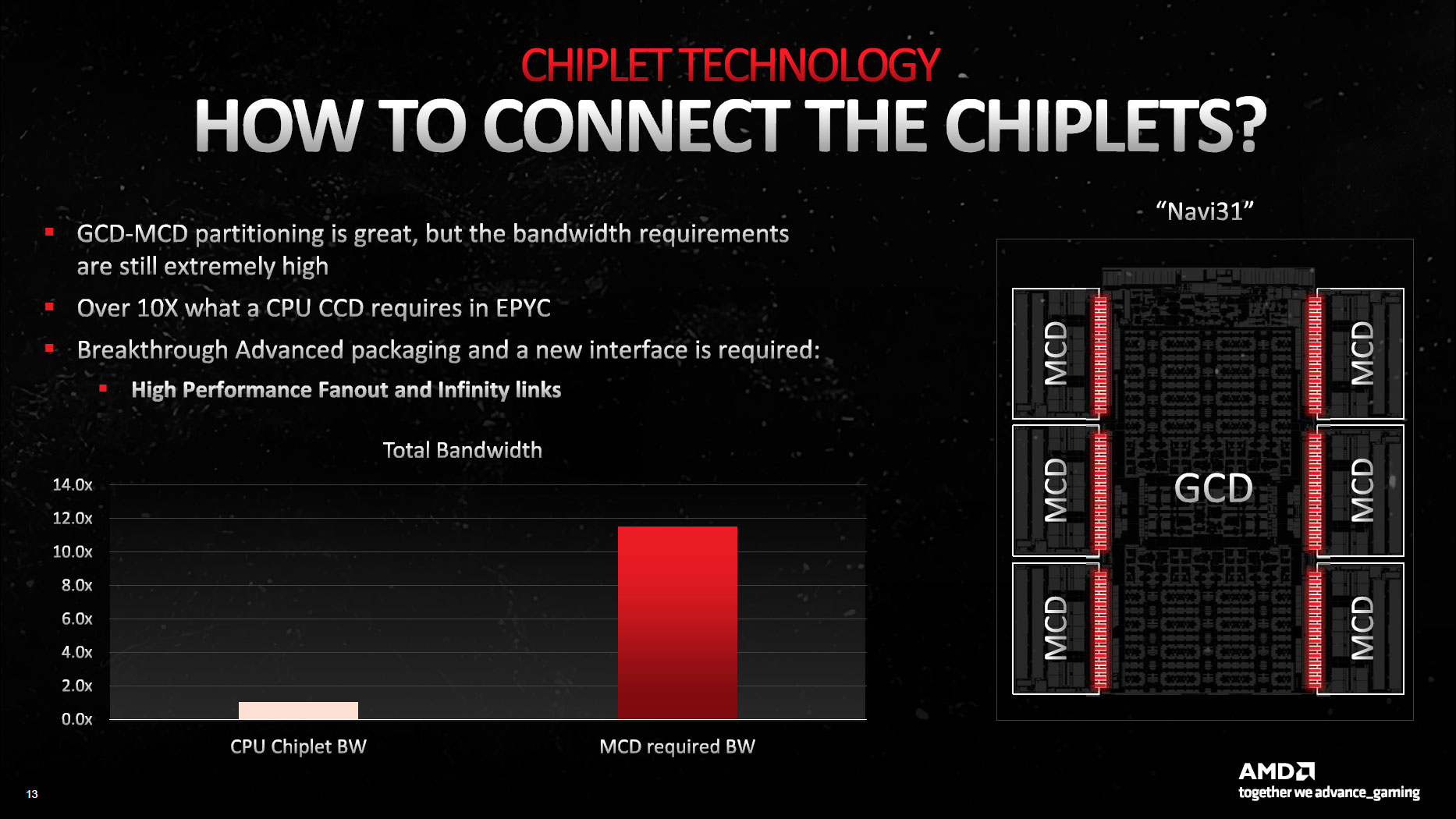
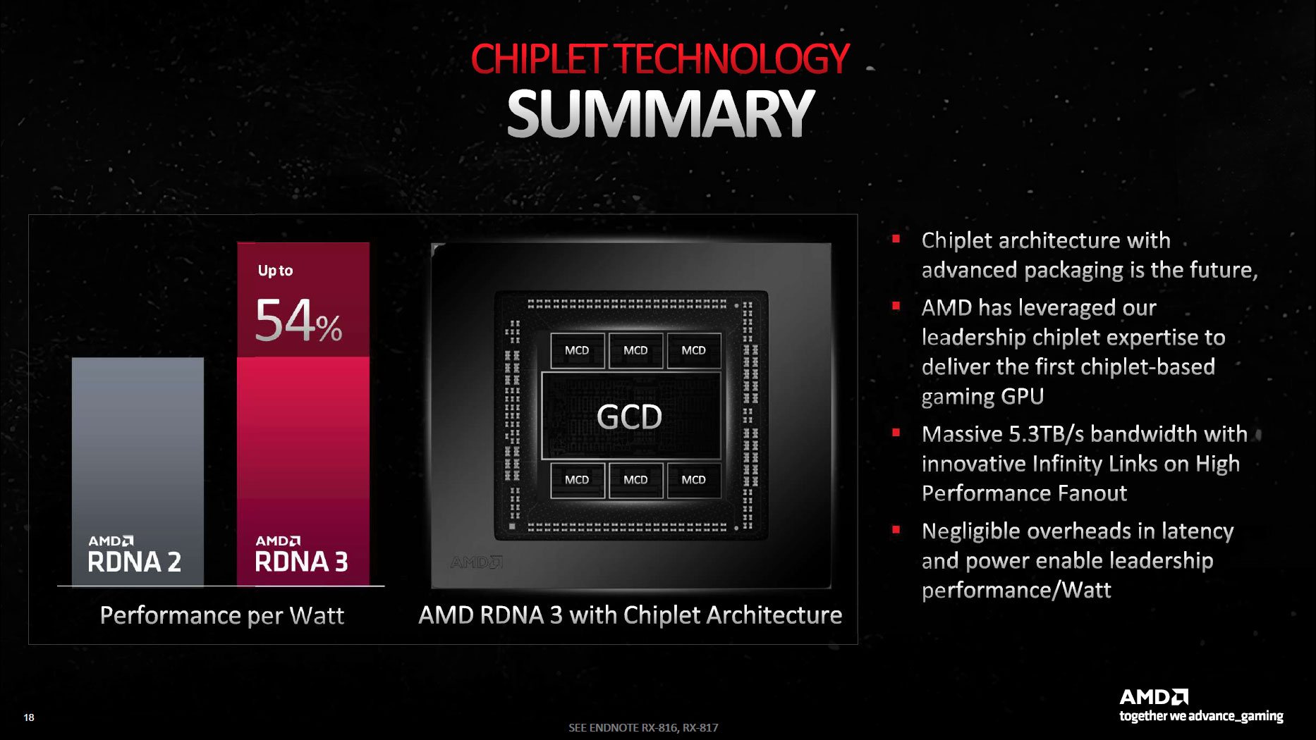
Navi 31 consists of two core pieces, the Graphics Compute Die (GCD) and the Memory Cache Dies (MCDs).
The GCD houses all the Compute Units (CUs) along with other core functionality like video codec hardware, display interfaces, and the PCIe connection. The Navi 31 GCD has up to 96 CUs, which is where the typical graphics processing occurs. But it also has an Infinity Fabric along the top and bottom edges (linked via some sort of bus to the rest of the chip) that then connects to the MCDs.
The MCDs, as the name implies (Memory Cache Dies) primarily contain the large L3 cache blocks (Infinity Cache), plus the physical GDDR6 memory interface. They also need to contain Infinity Fabric links to connect to the GCD, which you can see in the die shot along the center facing edge of the MCDs.
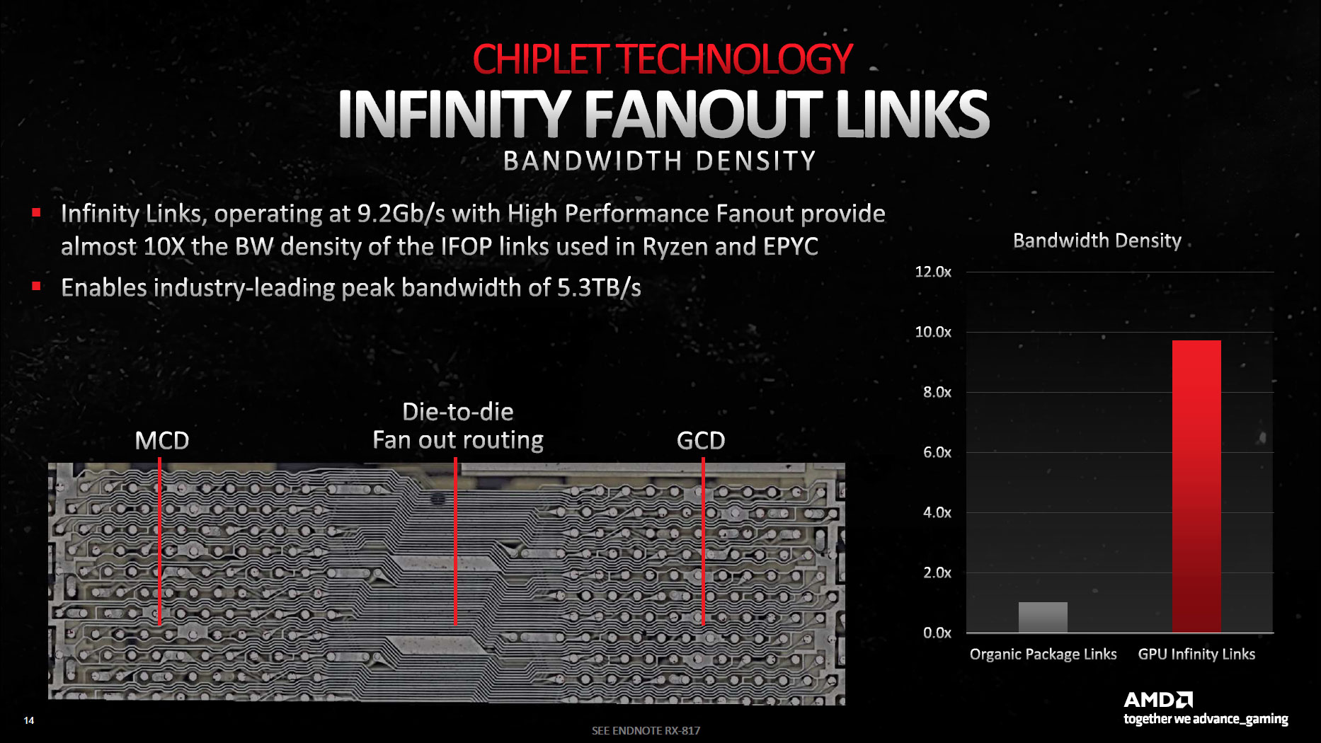
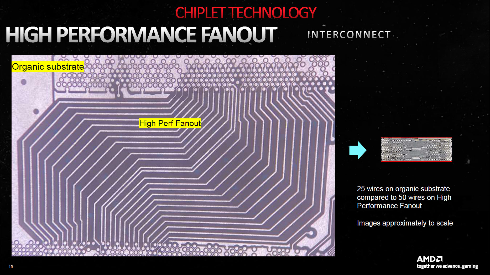
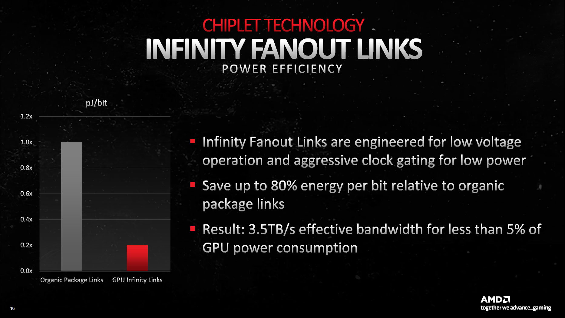
The result is what AMD calls the high performance fanout interconnect. The image above doesn't quite explain things clearly, but the larger interface on the left is the organic substrate interconnect used on Zen CPUs. To the right is the high performance fanout bridge used on Navi 31, "approximately to scale."
You can clearly see the 25 wires used for the CPUs, while the 50 wires used on the GPU equivalent are packed into a much smaller area, so you can't even see the individual wires. It's about 1/8 the height and width for the same purpose, meaning about 1/64 the total area. That, in turn, dramatically cuts power requirements, and AMD says all of the Infinity Fanout links combined deliver 3.5 TB/s of effective bandwidth while only accounting for less than 5% of the total GPU power consumption.
RDNA 3 Architecture Upgrades
That takes care of the chiplet aspect of the design, so now let's go into the architecture changes to the various parts of the GPU. These can be broadly divided into four areas: general changes to the chip design, enhancements to the GPU shaders (Stream Processors), updates to improve ray tracing performance, and improvements to the matrix operation hardware.
Another point AMD makes is that it has improved silicon utilization by approximately 20%. In other words, there were functional units on RDNA 2 GPUs where parts of the chip were frequently sitting idle even when the card was under full load. Unfortunately, we don't have a good way to measure this directly, so we'll take AMD's word on this, but ultimately this should result in higher performance.
Compute Unit Enhancements
Outside of the chiplet stuff, many of the biggest changes occur within the Compute Units (CUs) and Workgroup Processors (WGPs). These include updates to the L0/L1/L2 cache sizes, more SIMD32 registers for FP32 and matrix workloads, and wider and faster interfaces between some elements.
AMD's Mike Mantor presented the above and the following slides, which are dense! He basically talked non-stop for the better part of an hour, trying to cover everything that's been done with the RDNA 3 architecture, and that wasn't nearly enough time. The above slide covers the big-picture overview, but let's step through some of the details.
RDNA 3 comes with an enhanced Compute Unit pair — the dual CUs that became the main building block for RDNA chips. A cursory look at the above might not look that different from RDNA 2, but then notice that the first block for the scheduler and Vector GPRs (general purpose registers) says "Float / INT / Matrix SIMD32" followed by a second block that says "Float / Matrix SIMD32." That second block is new for RDNA 3, and it basically means double the floating point throughput.
You can choose to look at things in one of two ways: Either each CU now has 128 Stream Processors (SPs, or GPU shaders), and you get 12,288 total shader ALUs (Arithmetic Logic Units), or you can view it as 64 "full" SPs that just happen to have double the FP32 throughput compared to the previous generation RDNA 2 CUs.
This is sort of funny because some places are saying that Navi 31 has 6,144 shaders, and others are saying 12,288 shaders, so I specifically asked AMD's Mike Mantor — the Chief GPU Architect and the main guy behind the RDNA 3 design — whether it was 6,144 or 12,288. He pulled out a calculator, punched in some numbers, and said, "Yeah, it should be 12,288."
Along with the extra 32-bit floating-point compute, AMD also doubled the matrix (AI) throughput as the AI Matrix Accelerators appear to at least partially share some of the execution resources. New to the AI units is BF16 (brain-float 16-bit) support, as well as INT4 WMMA Dot4 instructions (Wave Matrix Multiply Accumulate), and as with the FP32 throughput, there's an overall 2.7x increase in matrix operation speed.
That 2.7x appears to come from the overall 17.4% increase in clock-for-clock performance, plus 20% more CUs and double the SIM32 units per CU. (But don't quote me on that, as AMD didn't specifically break down all of the gains.)
Bigger and Faster Caches and Interconnects
The caches, and the interfaces between the caches and the rest of the system, have all received upgrades. For example, the L0 cache is now 32KB (double RDNA 2), and the L1 caches are 256KB (double RDNA 2 again), while the L2 cache increased to 6MB (1.5x larger than RDNA 2).
The link between the main processing units and the L1 cache is now 1.5x wider, with 6144 bytes per clock throughput. Likewise, the link between the L1 and L2 cache is also 1.5x wider (3072 bytes per clock).
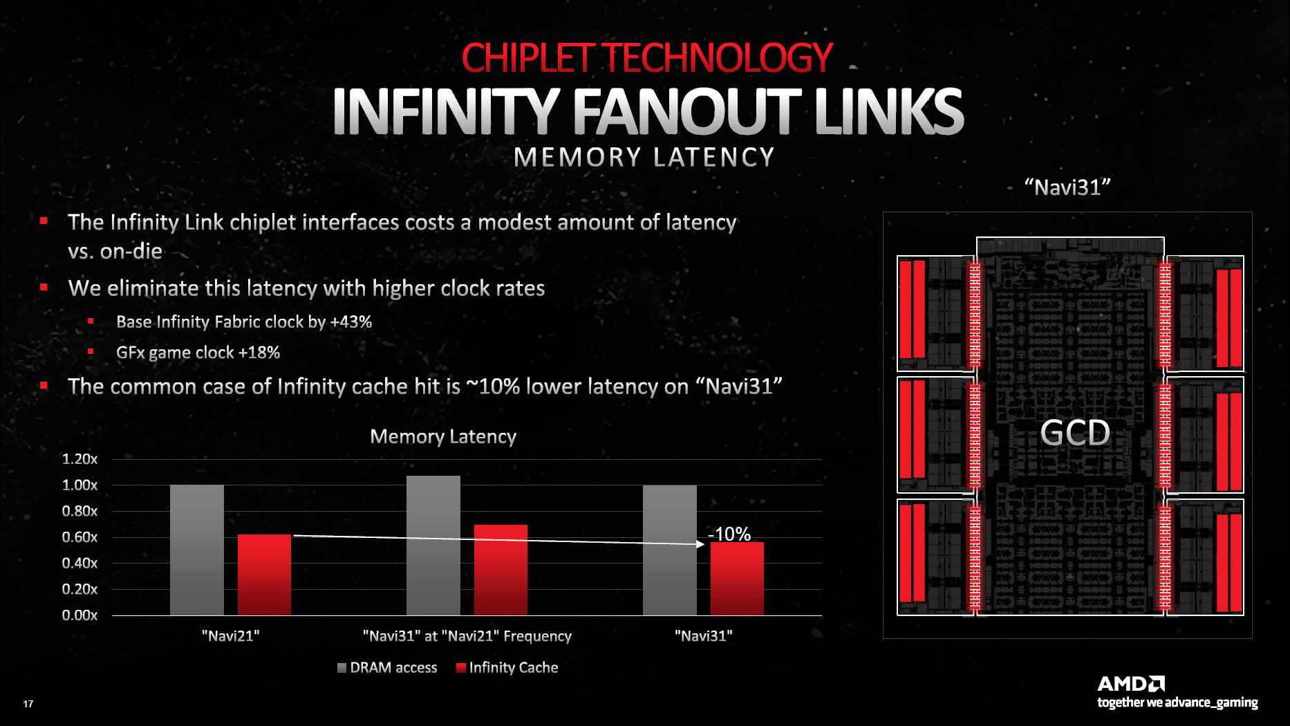
The L3 cache, also called the Infinity Cache, did shrink relative to Navi 21. It's now 96MB vs. 128MB. However, the L3 to L2 link is now 2.25x wider (2304 bytes per clock), so the total throughput is much higher. In fact, AMD gives a figure of 5.3 TB/s — 2304 B/clk at a speed of 2.3 GHz. The RX 6950 XT only had a 1024 B/clk link to its Infinity Cache (maximum), and RDNA 3 delivers up to 2.7x the peak interface bandwidth.
Note that these figures are only for the fully configured Navi 31 solution in the 7900 XTX. The 7900 XT has five MCDs, dropping down to a 320-bit GDDR6 interface and 1920 B/clk links to the combined 80MB of Infinity Cache. We will likely see lower-tier RDNA 3 parts that further cut back on interface width and performance, naturally.
AMD 2nd Generation Ray Tracing
Ray tracing on the RDNA 2 architecture always felt like an afterthought — something tacked on to meet the required feature checklist for DirectX 12 Ultimate. AMD's RDNA 2 GPUs lack dedicated BVH traversal hardware, opting to do some of that work via other shared units, and that's at least partially to blame for their weak performance.
RDNA 2 Ray Accelerators could do up to four ray/box intersections per clock, or one ray/triangle intersection. By way of contrast, Intel's Arc Alchemist can do up to 12 ray/box intersections per RTU per clock, while Nvidia doesn't provide a specific number but has up to two ray/triangle intersections per RT core on Ampere and up to four ray/triangle intersections per clock on Ada Lovelace.
It's not clear if RDNA 3 actually improves those figures directly or if AMD has focused on other enhancements to reduce the number of ray/box intersections performed. Perhaps both. What we do know is that RDNA 3 will have improved BVH (Bounding Volume Hierarchy) traversal that will increase ray tracing performance.
RDNA 3 also has 1.5x larger VGPRs, which means 1.5x as many rays in flight. There are other stack optimizations to reduce the number of instructions needed for BVH traversal, and specialized box sorting algorithms (closest first, largest first, closest midpoint) can be used to extract improved efficiency.
Overall, thanks to the new features, higher frequency, and increased number of Ray Accelerators, AMD says RDNA 3 should deliver up to a 1.8x performance uplift for ray tracing compared to RDNA 2. That should narrow the gap between AMD and Nvidia Ampere. Still, Nvidia also seems to have doubled down on its ray tracing hardware for Ada Lovelace, so we wouldn't count on AMD delivering equivalent performance to RTX 40-series GPUs.
Other Architectural Improvements
https://www.tomshardware.com/news/amd-rdna-3-gpu-architecture-deep-dive-the-ryzen-moment-for-gpus
"RDNA3" Instruction Set Architecture
https://developer.amd.com/wp-content/resources/RDNA3_Shader_ISA_December2022.pdf
Última edição pelo moderador: