Processador Intel Xeon Phi Knights Landing

Nemesis11

Power Member
Breaking down Intel’s upcoming Xeon Phi Knights series HPC platform.

Who would have thought that just a few years ago that the troubled Larrabee platform, which cost quite a few high level Intel executives dearly, would have been re-born so successfully within the high-performance computing (HPC) field as Xeon Phi? After all, Nvidia, and, with much lesser success, AMD, have already tried the GPGPU accelerator approach there, and real-world limitations of the heterogeneous computing software model issues led to less deployable apps than originally thought.

Intel did, and still does, have one huge comparative advantage in this situation: its broad x86 code compatibility. To put it simply, this allows inline programming from the same code base as usual Xeons which shortens the software optimized porting time from months to days, with associated costs savings. This was one off the reason why its first commercial Knights Corner model, precisely, 48,000 of them, found their way into Guangzhou’s Tianhe 2, the world’s fastest supercomputer. That machine will be expanded to its full 100 Peta flop (PFLOPS) original target capacity over the next year or so. NASA’s new supercomputer and a number of other large systems incorporate the Xeon Phi as well.

So, it is expected Intel would continue to nurture the new baby, and, in mid-2015, Knights Landing, the next generation Xeon Phi, is on the cards – with lots of changes.

1040091911.png


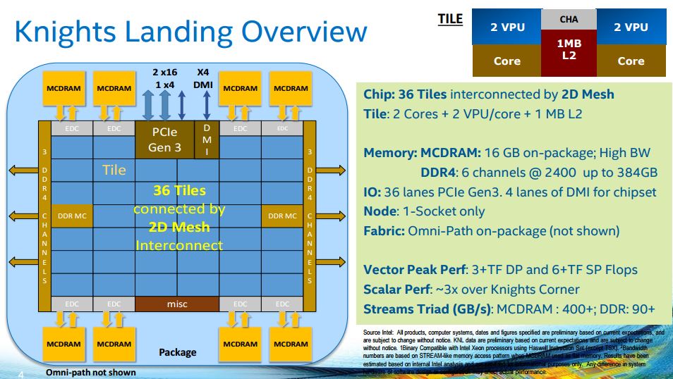
Quite simply, Knights Landing is a standalone CPU, just like any Xeon or Core Intel processor. It can boot the OS, connect to I/O bridges, have a direct HPC interconnect link to other Knights Landing and Xeon processors (Intel’s 100 Gbps Cray interconnect) and use the expandable main memory just like usual processors.

Each Knights Landing Xeon Phi has a 6-channel DDR4-2400 memory controller supporting up to 384 GB RAM per socket, a big improvement over the 16 GB seen in the current Xeon Phi. What about losing the GDDR5 bandwidth benefit, though? Well, there’s a bunch, up to 16 GB, of directly attached stacked 3D memory on top of the Knights Corner package at 500 GB/s bandwidth (over 50 percent faster), and with lower expected latency, than the top memory bandwidth of Tesla K40 or AMD R9-290X today.

1892917912.png


This memory can act either as a cache to the main RAM, or simply as the first 16 GB of the memory address space, whatever the specific environment prefers. Alternatively, you can design 4 GB of it as a cache and the remainder as the directly addressable memory.

There are also 36 PCIe v3 lanes for HPC interconnects, external GPU or local extra Knights Landing co-processor card connection, I/O bridges, SSD and so on.

The 72-core Knights Landing will use modified Atom Silvermont cores as the front end to the 512-bit wide vector units supporting AVX-512 instruction set. Silvermont, proven now in the mobile and microserver arena, has around twice the average efficiency of the old, 1997 Pentium-style in-order cores used in the first Xeon Phi.

1900945413.png


Knighs Landing promises over twice the performance of the current models: 6 TFLOPs single precision FP and, more importantly, 3 TFLOPs double precision FP per socket – the latter one counts more for productivity technical computing. Remember, AMD was cutting the DP FP rate in the R9 290 and 290X to 1/8 of SP compared to 1/4 of SP in the HD7970 to avoid competing with the future HPC accelerator flavor of R9-290X?

At over 3 TFLOPs per socket, and four sockets easily per each 1U in a rack, you could have half a petaflop in a usual 42U rack without using any special dense system packaging approaches. If relying on super dense, liquid cooled designs like Eurotech, fitted within a larger rack, a petaflop rack becomes possible on the X86 platform for the first time in 2015.

Now comes the icing on the cake. A quarter later, there will be a special packaging flavour, called Knights Landing-F, that will use Intel’s recently acquired and further developed low latency Cray HPC interconnect controllers, at 100 Gbit/s across two channels, connected via 32 of its PCIe v3 lanes, directly on top of the package with optical links coming out from there to the backplane switch.

It will help save a tiny bit of latency and some power too, but the unique approach of supercomputer interconnect links coming out directly from the CPU chip package towards thousands of other same CPUs (or Broadwell Xeon E5 v4 as well) is a breath of fresh air.

1082317614.png


Finally, towards the end of 2015, Knights Landing will still be also available as a PCIe co-processor card to the usual Xeon systems, although Intel’s card design only uses 2 out of 6 DDR4 channels for up to 64 GB RAM.

For the first time there would be an opportunity for third party OEMs to design improved Knights Landing cards with more RAM? Either way, it seems Intel prefers to offer the future Xeon Phi as stand-alone processors.

HPC is serious business

Intel is dead serious about capturing the dominant position in HPC accelerator market with the future iterations of Xeon Phi, and, even more importantly, creating Xeon Phi-only SIMD supercomputers for the first time, with petaflop-a-rack performance.

The usual serial and scalar jobs will still run better on ~1 TFLOPs 16-core Broadwell Xeon E5 v4 at the same time, but, well, at least there will be a choice of two approaches, or easy combining them into a single system with common code running on both.

Finally, aside from HPC, Knights Landing may be a ideal CPU for certain kinds of simulation-oriented heavily parallel games too. Just think of the possibilities.

http://vr-zone.com/articles/xeon-phi-knights-series-continues-landing-2015/64112.html

Então, o que temos aqui no Futuro Xeon Phi:
- Um processador completo que pode bootar um sistema operativo. Pode não funcionar como um coprocessador.
- 72 cores Atom/4 Threads por core. Parece-me que em vez de ser um ring a nível de disposição, é um mesh.
- Parece ter 1 MB L2 por cada 2 cores.
- 14 nm
- 2 unidades AVX-512 por core, compatíveis com outros cpus Intel com estas instruções, menos Transactional memory.
- 16 GB de stacked 3D Memory a 500 GB/s que podem funcionar de várias formas, como Ram ou cache.
- 6 controladores de memória que podem levar 384 GB de Ram por cpu, além da stacked Ram. DDR4-2400.
- 36 lanes Pci-Ex 3.0
- Integrated Fabric para comunicação a 100 Gbits, que ocupam 32 lanes Pci-Ex.
- Entre 160 a 215 W
- Previsão de 6 TFlops SP e 3 TFlops DP.

Parece-me interessante no mínimo. Não é nada que vá estar disponível para o consumidor, mas é uma montra de tecnologia.
Claro que visto o caminho que está a seguir a Intel, a nVidia não tem outra hipotese se não criar Teslas com processadores Arm integrados, para não precisarem de um cpu x86 agregado.
São tempos interessantes que aí vêm.
 
Última edição:
Mais um artigo sobre este processador:

http://www.realworldtech.com/knights-landing-details/

knl2-1.png


If the analysis is correct and Intel can execute on these plans, then Knights Landing will be a technical tour de force when it is released, probably in 2015. We estimate that Knights Landing will improve raw FLOP/s by >2.5×, but the most significant changes are in the memory hierarchy where cache bandwidth has jumped even more and the on-die capacity has increased by nearly a factor of 5. The single threaded performance will also be substantially higher with the move to the out-of-order core derived from Silvermont, enabling many more workloads to stay resident on Knights Landing. In fact, it is quite possible that the x86 core may be able to turbo to significantly higher frequencies when the vector units are inactive (e.g., on scalar, latency-sensitive code), further boosting single threaded performance.

The cost of all this performance is silicon die area. To date, the largest chip that Intel has manufactured in volume is Tukwila, which was a staggering 700mm2. Knights Landing is probably about the same size and possibly even bigger (if Intel has figured out how to increase the reticle limit). On top of that, the data arrays alone for 16GB of eDRAM are 1000mm2, once the control logic and I/Os are accounted for, that is likely to be 1200mm2 (albeit spread across multiple chips).

There are two clear takeaways. First, the level of investment is quite spectacular and demonstrates that Intel considers the HPC market to be absolutely vital and will not let Nvidia’s advances go unchecked. Second, the significant gains in performance are much larger than the 22nm to 14nm transition can explain; this implies that Knights Corner suffered from a number of challenges. The most reasonable theory is that the Knights Corner team was limited by the available resources and time to market. Knights Landing leverages Intel’s investments (e.g., eDRAM, Skylake fabric and uncore) much more intelligently and the overall product is much more closely tailored to the needs of the market.
 
Gostei desta eDRAM. Será que tem potencial para isso vir em consumer cpus? Ter 2 GB on package a 500 GB/s deve ser muito interessante.

Resta saber se é melhor ficar como RAM endereçavel ou funcionar como Cache L4
 
Gostei desta eDRAM. Será que tem potencial para isso vir em consumer cpus? Ter 2 GB on package a 500 GB/s deve ser muito interessante.

Resta saber se é melhor ficar como RAM endereçavel ou funcionar como Cache L4

Já tens eDRAM no mercado consumidor com os Haswell que têm a gráfica GT3e que têm 128 MB de eDRAM.
Apesar de o objectivo ser o de melhorar a performance da gráfica, a eDRAM nestes processadores funciona como cache L4.
Não têm é a mesma performance desta eDRAM.

Funcionar como Ram ou cache, parece-me que depende do workload.
O que me parece é que se o workload for muito maior a 16 GB de Ram, será melhor funcionar como cache L4. Se couber dentro dos 16 GB de Ram, parece-me melhor funcionar como Ram, sendo os primeiros 16 GB endereçáveis do sistema.
O objectivo será sempre usar o mais possível de eDRAM em vez de DDR4.
Reparar que eles neste processador não usam GDDR como é actualmente usado no Xeon Phi.
 
Mas lá está é usado como cache e de forma a colmatar a ausência de memoria dedicada pro GPU. E este "sabor" do Haswell não existe para socket 1150, apenas BGA. (i7-4770R)

daí o que dava jeito era mesmo algo com mais espaço e com esta rapidez. Claro que valores de 16 GB era possivel num desktop ordinário nem ter memória ram (até que ponto a Intel podia explorar tal opção e ter sistemas embebidos e muito mais compactos/baratos por não ter o bus externo de memória?)
 
Última edição:
A questão do socket é algo que não seja problema a nível de tecnologia. O problema é mais se um produto com a GT3e é "viável" no mercado desktop.
Melhor dizendo, a Intel está com olhos postos no mercado mobile e também penso que seja aí que a GT3e faça mais sentido.

Dito isto, se olharmos para a evolução dos cpus, com o aumento da sua complexidade, foram sendo adicionadas níveis de cache. Na board, depois integrado, L1, depois L2, L3.
Com a diminuição do custo, é bem possível que eDRAM passe a ser algo comum nestes produtos.


Há vários motivos porque acho interessante este Knigths Landing.
É cpu que está fora do alcance da maioria dos mortais e por isso mesmo quem gosta de informática, não lhe liga muito, no entanto é um processador que me parece que mostra algumas opções tomadas pela Intel que se vão reflectir noutros produtos mais "baixo de gama", sejam eles Xeons para servidores, sejam eles cpus para consumidores.

Um exemplo é o uso de eDRAM, mas há outros, como o AVX-512 e para mim a cereja no topo do bolo, a comunicação entre os cores numa rede ao contrario de ser em ring, algo que já tinha sido mostrado em dois processadores de teste. O Terasclale e o SCCC.
 
Desculpem por este desenterranço desta thread, mas decorreu a apresentação do Knights Landing.

Algumas fotos:
44225_03_details-intels-next-gen-knights-landing-platform_full.jpg


44225_04_details-intels-next-gen-knights-landing-platform_full.jpg


44225_06_details-intels-next-gen-knights-landing-platform_full.jpg


Um htop em linux:
44225_09_details-intels-next-gen-knights-landing-platform_full.jpg


Taking A Look Under The Knights Landing Hood

The starting point for the Knights Landing processor is the heavily modified Silvermont Atom core, which has been so changed that Sodani says that it would probably be more accurate to call it a Knights core. Because Intel has streamlined the Silvermont core radically, yet while maintaining full compatibility with the Xeon processors as far as Linux and Windows applications are concerned, there is room to put lots of AVX floating point processing oomph into the chip.

The basic Knights Landing component is called a tile, and each tile has two of those modified Silvermont cores, each with 32 KB of L1 instruction cache and 32 KB of L1 data cache. The cores are topped with a pair each of a custom 512-bit AVX vector unit, which supports all of the same floating point math instructions as the ones used in the Xeon chips even though they are not literally lifted out of the most current Xeons. With more than 60 cores, that means Intel is putting more than 120 of these AVX units on a core. ?That kind of power density is hard to attain, even with a Broadwell,? says Sodani. ?This is more efficient.?

The Knights core is an out-of-order processor, and both the integer and floating point units use this technique, which has been common on server-class processors for decades. The out of order depth of the Knights core is more than twice that of the Silvermont core, and those L1 caches are also bigger than that on the Silvermont chip. Those cores, by the way, are real cores and they can do real X86 work. They are not just setting up work for the AVX units, and this is one thing that makes Knights Landing a real server processor. ?Our single-thread performance is actually pretty respectable,? says Sodani.

Two of the cores with their dual AVX units each are linked to each other on the tile by a shared L2 cache that weighs in at 1 MB of capacity, and a hub chip links the tile to the other tiles on the die. The tiles are linked to each other over a 2D mesh, and it is this mesh that provides the cache coherency between the L2 caches on the die. With 60 cores, that is at least 30 MB of L2 cache, and with 72 cores max, if that is indeed the number, then Knights Landing would peek at 36 MB of L2 cache. The L2 caches are separate and private, but coherent across the mesh. In plain English, what that means is that an operating system will see this as one processor with one cache and one memory space. (Well, if you want to.)

The 2D mesh on the Knights Landing chip has two DDR4 memory controllers, and each one of the 2 GB near memory MCDRAM units has its own controller, too, which hangs off the end of the mesh. The way the routing works, all hub routers on the mesh can move along the Y axis and then the X axis on the grid, and always in that fashion, which helps Intel keep the contention on the mesh down to a minimum.

The interesting thing about the Knights Landing processor is that it will have three memory modes. The first mode is the 46-bit physical addressing and 48-bit virtual addressing used with the current Xeon processors, only addressing that DDR4 main memory. In the second mode, which is called cache mode, that 16 GB of near memory is used as a fast cache for the DDR4 far memory on the Knights Landing package. The third mode is called flat mode, an in this mode the 384 GB of DDR4 memory and 16 GB of MCDRAM memory are turned into a single address space, and programmers have to allocate specifically into the near memory. Intel is tweaking its compilers so Fortran can allocate into the near memory using this flat addressing mode.

You might be thinking, as we were, why Intel doesn?t create a two-socket version of Knights Landing. If one socket is good, why not two? Intel could, in theory, put QuickPath Interconnect ports on the Knights Landing chip and make a two-socket or even four-socket variant with shared memory across multiple sockets.

?Actually, we did debate that quite a bit, making a two-socket,? says Sodani, ?One of the big reasons for not doing it was that given the amount of memory bandwidth we support on the die ? we have 400 GB/sec plus of bandwidth ? even if you make the thing extremely NUMA aware and even if only five percent of the time you have to snoop on the other side, that itself would be 25 GB/sec worth of snoop and that would swamp any QPI channel.?

As is ever the way with systems, the bottleneck has shifted, and in this case from inside the chip to the point-to-point interconnect. For now, Intel is not supporting cache coherency across the Omni-Path fabric, either. Again, there is just so much memory bandwidth that such coherency would swamp the interconnect.

http://www.theplatform.net/2015/03/25/more-knights-landing-xeon-phi-secrets-unveiled/
http://www.tweaktown.com/news/44225/details-intels-next-gen-knights-landing-platform/index.html
http://www.eetimes.com/document.asp?doc_id=1326121

Confirmam-se os detalhes dos rumores. Entre 60 a 72 cores, AVX 512 bits, MCDRAM, etc.
Uma besta de processador.
 
Bem, isso deve ser um belo monstro de processamento :D

É um monstro a nível de processamento e o que é mais interessante é que é um computador completo em si mesmo. Tem cores x86, com DMI para ligar a um chipset, etc etc.
Está tudo integrado, ou quase tudo. É interessante também porque coloca a nVidia numa posição complicada. A nVidia aposta agora nas suas gráficas com Power da IBM. Não sei se vai fazer sentido para muitos clientes, tendo sistemas completos no Xeon Phi, x86.
 
Epá, não estou dentro destes sistemas de processamento, portanto preciso de fazer perguntas de burro :D Ou seja, remove a Nvidia e os seus sistemas de processamento da equação no que toca a simulação/processamento?
 
Epá, não estou dentro destes sistemas de processamento, portanto preciso de fazer perguntas de burro :D Ou seja, remove a Nvidia e os seus sistemas de processamento da equação no que toca a simulação/processamento?

Não. O que faz é ter uma vantagem sobre a nVidia a nível de integração e de custos.
Neste mercado a nVidia parece estar a apostar tudo nos Power. nVlink, etc. O cliente tem à escolha entre um computador que não precisa de acessórios e compatível com código x86 legacy ou entre um sistama Power com o seu ISA diferente de x86 que ainda precisa de placas acessórias e usar Cuda por cima delas.
A nível de integração e possivelmente custos, a Intel está a ganhar. Há outros pontos importantes nesta integração, como por exemplo integrar a rede no próprio Chip (100 Gb/s em cada uma das duas portas do omni-path), switchs omni-path com 48 portas em vez de 36 de Infiniband, etc.

Mas não retira a nVidia do caminho. Se é verdade que há muita coisa em x86, também é verdade que para aproveitar a 100% este Xeon Phi, é preciso recompilar e também é verdade que já há muito software escrito em Cuda.

Neste mercado os próximos tempos serão interessantes. :)
 
Optimization Tests Confirm Knights Landing Performance Projections

NERSC Engineer in the Advanced Technologies Group, Douglas Doerfler, says there are consistencies between what Intel targeted with Knights Landing (KNL) compared to two-socket Haswell machines (as there will be in the “Cori” system once a pending upgrade is complete—the teams already have some KNL nodes). “We are seeing anywhere from equal performance to Haswell to 2-2.5X performance improvement.”
http://www.nextplatform.com/2016/07...firm-knights-landing-performance-projections/

O estudo completo
https://crd.lbl.gov/assets/Uploads/ixpug16-roofline.pdf


Um artigo que resume a experiência de várias instituições com o KL
http://www.nextplatform.com/2016/07/12/knights-landing-will-waterfall-high/
 
Última edição:
Parece que a intel está finalmente a colocar a lápide nesta gama:

Intel Begins EOL Plan for Xeon Phi 7200-Series ‘Knights Landing’ Host Processors

provavelmente deve ser replacement pelos GPUs que estão a desenvolver.

Acho que não tem qualquer relação. É normal que retirem do mercado o "Knights Landing" porque lançaram o "Knights Mill" que é basicamente a mesma coisa + suporte FP16.

Tendo em conta o roadmap do Aurora (A21), penso que o substituto directo do Phi não será um GPU mas o Cooper Lake AP/Icelake AP/etc.
Claro que esses não serão os únicos chips da Intel para o mercado de computação. Provavelmente terão também os GPUs, os ASICs da "Nervana", os FPGAs da "Altera", etc etc.
 
Com a Nvidia a dar forte com a Volta no mercado HPC/deep learning não é caso para dizer que a Intel está em apuros nisso?
 
Back
Topo