
GlobalFoundries 14 nm LPP FinFET Node Taped Out, Yields Good
Excelentes noticias!!
Excelentes noticias!!
http://www.eetimes.com/document.asp?doc_id=1327709&page_number=2Jha: You’re right. We’ve been a quarter or two late on the leading-edge nodes. That’s one of the issues we’ve been trying to address. Today, we have one 14nm customer ramping to volume right now, followed by two others who will be ramping later this year and early next year. That’s not too bad. When it comes to 14nm volume production, I think we are roughly on par with our competitors.
https://www.semiwiki.com/forum/content/5119-globalfoundries-14nm-process-update.htmlThe 14LPE process was the first generation and was qualified in January. A second generation 14LPP process was qualified in September. They are now shipping 14nm parts to customers.
...
Production qualification is greater than 60% yield on a 128Mb SRAM. Yields on LPP are >20 points higher than that now (>80%) and LPE is ahead of that.
http://www.globalfoundries.com/news...logy-success-for-next-generation-amd-productsAMD has taped out multiple products using GLOBALFOUNDRIES’ 14nm Low Power Plus (14LPP) process technology and is currently conducting validation work on 14LPP production samples. Today’s announcement represents another significant milestone towards reaching full production readiness of GLOBALFOUNDRIES’ 14LPP process technology, which will reach high-volume production in 2016.
http://www.globalfoundries.com/news...ies-expands-to-meet-worldwide-customer-demandGF plans to expand 14nm FinFET capacity by an additional 20 percent at its Fab 8 facility in New York, with the new production capabilities to come online in the beginning of 2018.
The Defense Microelectronics Activity, a branch of DoD’s laboratory network, last week awarded a $10.27 billion contract modification to eight vendors under a streamlined technology acquisition program. The award boosts the total for electronics engineering and manufacturing under the Advanced Technology Support Program (ATSP) to as much as $17.47 billion.
Vendors include some of the largest U.S. military contractors: Boeing, General Dynamics, Honeywell, Lockheed Martin, Northrop Grumman Systems and Raytheon Co.
https://www.eetimes.com/dod-microel...?utm_source=eetimes&utm_medium=relatedcontentGlobalFoundries serves as the office’s trusted foundry under a contract that extends through September 2023.
https://www.eetimes.com/trusted-dod-fabs-gloflo-skywater-join-forces/The foundry agreement follows a $170 million DoD contract award to SkyWater last October that funds a multi-phase project to manufacture radiation-hardened chips for military and aerospace customers. The initial $80 million phase includes development of a 90-nm rad-hard electronics manufacturing capability.

https://www.globalfoundries.com/new...cquire-land-malta-ny-positioning-its-advancedThe land parcel is located at the southeast end of the New York State Energy Research and Development Authority (NYSERDA) Saratoga Technology + Energy Park (STEP) campus, adjacent to Stonebreak Road Extension, between GF’s Fab 8 facility and Hermes Road. Exercising the option to purchase the land and commencement of development to expand GF’s Fab 8 facility will be subject to zoning regulations and client demand.
 )
)12LP+ builds upon GF’s established 14nm/12LP platform, of which GF has shipped more than one million wafers.
Driving the enhanced performance of 12LP+ are features including a 20-percent SoC-level logic performance boost over 12LP, and a 10-percent improvement in logic area scaling. These advancements are achieved in 12LP+ through its next-generation standard cell library with performance-driven area optimized components, single Fin cells, a new low-voltage SRAM bitcell, and improved analog layout design rules.
12LP+, a specialized application solution, is augmented by GF’s AI design reference package, as well as GF’s co-development, packaging, and post-fab turnkey services – which together enable a holistic experience for designing low-power, cost-effective circuits optimized for AI applications.
https://www.globalfoundries.com/new...ator-applications-globalfoundries-12lp-finfetIn addition to 12LP’s existing IP portfolio, GF will expand the IP validations for 12LP+ to include PCIe 3/4/5 and USB 2/3 to host processors, HBM2/2e, DDR/LPDDR4/4x and GDDR6 to external memory, and chip-to-chip interconnect for designers and clients pursuing chiplet architectures.
Wait, eles vêm para a Europa para produzir? Percebi bem?
After a few years of conducting simulation-based explorations into 3D-ICs, Arm Research decided that these questions could best be answered by building a demonstrator. This required a strong collaboration between design, electronic design automation (EDA), and manufacturing.
To make that demonstrator a reality, Arm partnered with GLOBALFOUNDRIES to tape-out a 3D prototype design in 2019. Named Project Trishul, the goal was to demonstrate the feasibility and readiness of high-density, face-to-face, wafer-bonded 3D stacking technologies for high performance, energy-efficient designs. Figure 1 shows the piece of a representative Arm Neoverse® system the team investigated, and a block diagram of the subsystem components that were demonstrated in 3D. We are happy to announce that the 3D hybrid-bonded chips are back from fabrication, and we have run comprehensive tests to measure and characterize them.
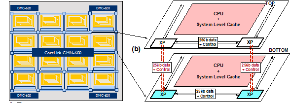
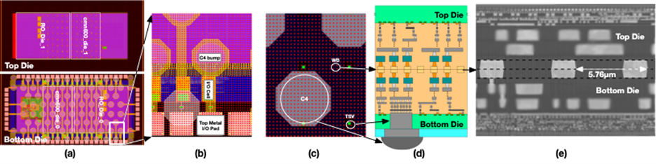
https://community.arm.com/developer...ion-high-performance-energy-efficient-systemsThe key learning that we validated from this 3D test-vehicle was that, from an electrical-connectivity perspective, face-to-face hybrid bonding technology does not introduce any significant delay penalty. If the cross-die process skew can be managed, a single clock domain synchronous design with an order of magnitude higher bandwidth and lower energy, compared to state-of-the-art bump-based die stacking techniques, can be implemented. 3D stacking can significantly improve on-chip memory capacity and bandwidth, and can also improve the overall throughput of the system, all while potentially reducing costs.