Processador Curiosidades de hardware

China's Phytium Launches 64-Core Server CPUs, Despite Spot on US Entity List​

Yet despite sanctions, the company is still in business, and this week it introduced its first 64-core Feiteng Tengyun S2500 processor for datacenter applications at the Global Memory Industry Innovation Forum 2023.

Phytium's Feiteng Tengyun S2500 is a 64-core processor based on the company's proprietary (and rather outdate) FTC661 cores that rely on the Armv8 instruction set architecture. The processor is specifically designed for cloud and high-performance computing applications and is essentially a superset of the company's FT-2000+/64 processor from 2021. The Feiteng S2500 adds a large-capacity shared L3 cache, four direct connection ports boasting a total bandwidth of 800Gbps, revamped security capabilities for cloud servers, and a more reliable memory subsystem.
https://www.tomshardware.com/news/c...re-server-cpus-despite-spot-on-us-entity-list

Para já nenhuma menção ao processo de fabrico e Foundry usada, mas o dito SoC aparentemente foi testado por uma das empresas da cloud/comércio online chinesa durante um evento em Junho

The domestic Phytium CPU can carry JD 618! The only eight-way 512 core, performance soared by 50%​

Fast Technology News on June 20, in the JD.com 618 shopping festival that just passed, the domestic Phytium CPU successfully provided the core computing power support and passed the technical test smoothly. This is after the large-scale application of government affairs, electric power, transportation, finance, telecommunications and other fields, Phytium CPU has also achieved large-scale application in consumer markets such as e-commerce platforms, so that localization can be used for real purposes. Statistics show that within 10 minutes after the start of JD 618 this year, the peak user visits per second of JD Cloud increased by 112% year-on-year. The ever-increasing peak data poses severe challenges to JD Cloud’s service architecture and underlying computing power. More than 1,000 servers with Feiteng Tengyun S2500 CPU as the computing power base provide full-stack product support for JD Cloud, covering all link scenarios.
https://www.gamingdeputy.com/the-do...-eight-way-512-core-performance-soared-by-50/
 

AYANEO announces Nintendo DS inspired “Flip DS” handheld, Macintosh and NES inspired “Retro” Mini-PCs​


AYENEO-REMAKE-e1699609435134-1200x542.jpg

https://videocardz.com/newz/ayaneo-...eld-macintosh-and-nes-inspired-retro-mini-pcs
 

Google Brings TPU v5e AI Board to SC23​


Google brought its new TPU v5e to SC23 in Denver. It is uncommon for Google to bring this new hardware to events, and so the company has a security guard around the board. We managed to grab a few photos last evening of Google’s cloud AI board so other folks not at the show can see.
Google-TPU-v5e-Interconnects-and-Heatsinks-696x506.jpg

Google-TPU-v5e-Heatsink-696x524.jpg

Google-TPU-v5e-Side-Angle-696x486.jpg

Google-TPU-v5e-Overhead-696x517.jpg

Google published a TPU v5e video where it showed this assembly without the heatsinks.
Google-TPU-v5e-Without-Heatsinks-1-1-696x476.jpg

Google-TPU-v5e-Without-Heatsinks-2-1-696x342.jpg

https://www.servethehome.com/google-brings-tpu-v5e-ai-board-to-sc23/
 
No Microsoft Ignite além do Cobalt 100 (ARM core CPU) ambém anunciaram um AI chip - o Azure Maia 100, apresentado como "GPU", mas nesse os pormenores ainda são mais escassos.

Microsoft Reveals Custom 128-Core Arm Datacenter CPU, Massive Maia 100 GPU Designed for AI​

What we do know is that the Maia 100 AI Accelerator - a GPU - is designed for large language models. Microsoft says that OpenAI "provided feedback" about the Maia 100 designs.
The company also states that designing its own chips allows it to increase cooling in data centers and to boost the capacity in existing facilities. The company said that there were no server racks that could "house the unique requirements of the Maia 100 server boards," which required building racks from scratch.

"These racks are wider than what typically sits in the company’s datacenters," Microsoft's blog post reads. "That expanded design provides ample space for both power and networking cables, essential for the unique demands of AI workloads."
DvyDnhbF3gHu3p5dR3bSgX.jpg

GBkCY858j58RYathYtkKfW-970-80.jpg

The company also needed to come up with a liquid cooling solution to chill these chips during complex AI tasks, but didn't have data centers set up for "large liquid chillers." So Microsoft is using what it calls a "sidekick" that can sit next to a rack of Maia 100 servers, send cold liquid to cold plates attached to the Maia 100 chips, and then send the warm liquid back to the sidekick to remove the heat and return the liquid to the rack again.
https://www.tomshardware.com/news/microsoft-azure-maia-ai-accelerator-cobalt-cpu-custom


Microsoft Holds Chip Makers’ Feet To The Fire With Homegrown CPU And AI Chips​

Here is the Maia 100 AI accelerator chip that Nadella held up:
microsoft-ignite-maia-100-chip-shot.jpg

What we can tell you is that the Maia 100 chip is based on the same 5 nanometer processes from TSMC and includes a total of 105 billion transistors, according to Nadella. So it is no lightweight when it comes to transistors or clock speed. The Maia 100 chip is direct liquid cooled and has been running GPT 3.5 and is powering the AI copilot that is part of GitHub right now. Microsoft is building up racks with the Maia 100 accelerators and will be allowed to power outside workloads through the Azure cloud next year.
https://www.nextplatform.com/2023/1...-to-the-fire-with-homegrown-cpu-and-ai-chips/
 
Última edição:

Apple-Scented Thermal Paste Launches in Japan​

A new limited edition apple-scented thermal paste was launched in Japan today. A collaborative effort between M1N1ing and Clock Work Tea Party, the Extreme Muglis 4G Apple Edition EG4GAP paste is formulated for room-temperature overclocking antics. No, this isn’t designed for Apple's Mac computers, it just reportedly smells like an Apple and comes in green.

The thermal paste was first reported by Japanese publication Hermitage Akihabara. While it doesn't offer a reasoning for the scent, the idea behind the suitably apple green color is that it contrasts better with the silver metal IHS which caps a processor, making it easier to ensure even and complete coverage.
In some supplemental information about the quality of the new CWTP-EG4GAP paste, it is described as using extremely fine particles precipitated using ultrasonic technologies. Considering the specs, its 12.8 W/mk thermal conductivity is a smidgeon better than the well-regarded Thermal Grizzly Kryonaut. However, we can’t say anything about the actual performance, ease of use, or cleanup of EG4GAP, without some testing time.

The Extreme Muglis 4G Apple Edition EG4GAP paste is going to be a limited release of 1,000 syringes.
Bfgdiwu.jpg


wg2wVwo.jpg


UQwMiYQ.jpg


FcvljqB.jpg

https://www.gdm.or.jp/pressrelease/2023/1117/514492

Japão sempre em grande. :D
 

:n1qshok:

New Chinese chip uses IBM's open source Power ISA instead of x86 or Arm — country searches for alternatives to sanctioned US processor designs as firm debuts second-gen server CPU​

Most server CPUs today use the Arm, RISC-V, or x86 instruction set architecture (ISA), but the Hexin team has turned to IBM's Power, an open source RISC ISA. This ISA is formally open to everyone and debuted in China in 2014. The Hexin team comprises 400 members, many recruited from IBM's high-performance R&D center. The team has "reconstructed" IBM's closed design methodology with its EDA chip design tools, design flow, and architecture.
Hexin's HX-C2000 server design features an unknown number of RISC cores and appropriate input/output capabilities. Before Hexin builds its fully-fledged HX-C2000, it must build test chips (TC). The initial TC1 version was taped out and powered in 2022, and recently, the company powered on its second test chip, the TC2 (HX-C2000TC2). Apparently, it took Hexin just four hours to power on its HX-C2000TC2, indicating the silicon's readiness. In addition, the developer claims the chip met all of its expectations.
https://www.tomshardware.com/news/c...com&utm_medium=social&utm_campaign=socialflow
 

Huawei's sanctions-evading Kirin 9000S processor tested: significantly behind its Kirin 9000 predecessor that used TSMC tech​


The year was 2020, and Huawei released its HiSilicon Kirin 9000, an application processor for smartphones that used TSMC's N5 (5nm-class) process technology and packed 15.3 billion transistors — just before the company got listed on the Entity List of the U.S. government and lost access to TSMC. In 2023, the company launched its Kirin 9000S: a version of the Kirin 9000 made by SMIC using its 2nd-gen 7nm-class process technology. Nanoreview.net this week tested the new system-on-chip and its verdict was not exactly favorable.
The new Huawei HiSilicon Kirin 9000S processor can keep up and even leave behind its predecessor when it comes to general-purpose CPU workloads, but when it comes to power efficiency and graphics workloads, it is considerably behind the Kirin 9000 that is now more than three years old. The results are not particularly surprising as it is hard to beat a 5nm processor with a 7nm SoC unless you sacrifice power efficiency and cost.

Nanoreview.net tested both the original Kirin 9000 and the Kirin 9000S in popular benchmarks, including AnTuTu 10, Geekbench 6, 3DMark Wild Life, and numerous mobile games.
zJ2PG4iFzBWXW3yiaysLX.png

Huawei's HiSilicon Kirin 9000S demonstrated a similar total score (around 900,000 points) to the original Kirin 9000 in AnTuTu 10, but it was 33% behind in GPU performance than its ancestor. Surprisingly, despite lower clocks and the same core count, the Kirin 9000S was 4% faster in the single-thread Geekbench 6 workload and 17% faster in the multi-thread Geekbench 6 workload. The Kirin 9000 is also 20% faster than the Kirin 9000S in 3DMark Wild Life, which is probably because the company could not build a GPU that would be as fast as a 24-cluster Arm Mali-G78 (1536 stream processor) working at 759 MHz.
https://www.tomshardware.com/pc-com...ignificantly-behind-kirin-9000-with-tsmc-tech
 

Geely’s Dragon Eagle-1 first China-made automotive-grade chip is on more than 200,000 vehicles​

On December 25, SiEngine announced that its Dragon Eagle-1 automotive-grade 7-nanometer cockpit chip is now on more than 200,000 vehicles since the chip’s first release in December 2021. So far, Dragon Eagle-1 can be found on the Lynk & Co 08 SUV, Lynk & Co 06 EM-P SUV, and Livan 7 SUV, which are all part of the Geely Auto Group; and has received orders from other manufacturers including FAW for more than 20 vehicle models.
Dragon Eagle-1 is China’s first automotive-grade 7-nanometer system-on-chip (SoC) cockpit chip, which is an integrated circuit that compresses all of a system’s required components onto one chip. As small as the size of a fingernail (83 mm²), it has 8.8 billion transistors and 87 layers of circuits. In layman’s terms, that is equivalent to 8.8 billion small houses and 87 floors. Furthermore, Dragon Eagle-1 has an 8-core CPU, 14-core GPU, programmable NPU, ISP, VPU, and DSP clusters.
image-18-800x649.png


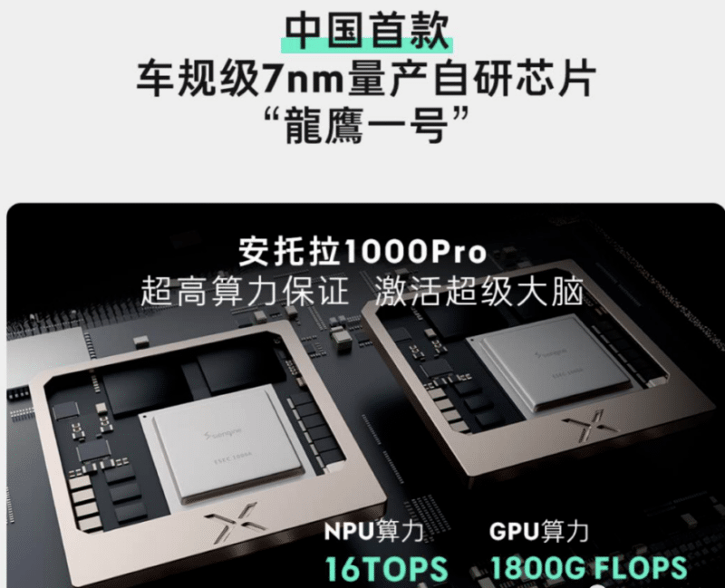
The company behind the Dragon Eagle-1 chip is SiEngine, which is a joint venture between ECARX and ARM China, established in the Wuhan Economic and Technological Development Zone in September 2018, dedicated to the design, development, and sales of advanced automotive electronic chips, according to the company website. ECARX is an automotive technology provider co-founded by Eric Li (Li Shufu), who is also the founder and chairman of Geely, in 2017. ARM is a chip design company under Softbank, headquartered in Cambridge, UK. As of June 30, 2022, ECARX held a 30.97% equity interest in SiEngine. As SiEngine’s important shareholders, ECARX and ARM China also provided core support for SiEngine’s early IP design and tape-out.
https://carnewschina.com/2023/12/25...e-grade-chip-is-on-more-than-200000-vehicles/
 

STMicroelectronics makes a 18K Big Sky Sensor So Large Only Four on a 300mm Wafter​


Just for some sense of the size, here is a side-by-side of the Big Sky sensor next to a DSLR sensor.
Big-Sky-Side-By-Side-Compare-Credit-STMicroelectronics-.jpg

The sensor itself measures around 8.31cm by 9.92cm. ST Micro designed and built the custom sensor during the pandemic so it could be tested and used to shoot for the the Sphere’s launch.
Big-Sky-Sensor-Spec-Credit-STMicroelectronics-.jpg

For some sense on how big this is, only four of these sensors can fit on a 300mm wafer.
Big-Sky-Sensor-Wafer-Credit-STMicroelectronics-copy-696x559.jpg

The 316MP sensor is designed to capture video at up to 120fps. With such a high resolution and framerate, the sensor can push around 60GB/s of image data. That requires multiple high-speed optical connections and a custom storage solution. For some sense, a standard 4TB external SSD cannot handle that much data ingest from a speed perspective, and it would be filled after around 67 seconds of footage was shot.
https://www.servethehome.com/stmicr...-sensor-so-large-only-four-on-a-300mm-wafter/
 
Acho curioso isso de fabricação de chips que tens os dies funcionais e montes de "bocados" nas bordas, neste caso tem 12 sensores incompletos.

E isso também ocorre em CPUs e GPUs, existe dies incompletos pelas orlas...

Não se faz o "mask" só dar "infuse" dos 4 sensores no centro, com o resto ser apenas silício in natura?
 
Última edição:
Acho curioso isso de fabricação de chips que tens os dies funcionais e montes de "bocados" nas bordas, neste caso tem 12 sensores incompletos.

E isso também ocorre em CPUs e GPUs, existe dies incompletos pelas orlas...

Não se faz o "mask" só dar "infuse" dos 4 sensores no centro, com o resto ser apenas silício in natura?

Estava a pensar exactamente no mesmo.
Aliás, até dá a ideia que se puxassem bem para a direita/esquerda quase que cabiam 6 lado a lado.

(não estou de todo a dizer que os engenheiros são parvos, mas algum motivo deverá haver)
 
Última edição pelo moderador:
Puxar pra direita não ia adiantar de muito, já está quase na borda e relembe que quanto mais perto da borda, pior qualidade terá.
 
Este deve ser dos Sistemas mais obscuros da Sega. Sega AI Computer.
"AI" já fazia vender computadores nos anos 80. :D Mais a sério, a ligação com "AI" parece ser feita pelo suporte de Prolog, que não chego a perceber onde é que usado. Parece ter tido como alvo o mercado educativo.

0v4CuhR.jpg


QXyeIEh.jpg


PQUQzKB.jpg


5C1RlnI.jpg


TK7LHkL.jpeg


Uanl8H6.png


S3U2g5r.jpeg


l508Col.png


Around late 1986, Sega released the “Sega AI Computer”. This is one of Sega’s least well known and rarest systems. Not much is known about this system apart from a small amount of information in Japanese and American flyers and press articles. The information we have is still piecemeal and may be partly inaccurate.

Today we are making public, for the first time: all system roms extracted from the Sega AI Computer, data dumps from 26 my-cards and 14 tapes, many scans and photographs, and in collaboration with MAME developers, an early working MAME driver allowing this computer to be emulated.

The majority of these software titles had zero information about them on the internet prior to us publishing them: no screenshots, no photos or scans of actual software. Considering the elusive nature of this machine, it is possible that some games have never been seen or completed by anyone outside of their original development teams.

System Specs​

  • Year: 1986
  • CPU: 16-bit NEC V20 at 5 Mhz
  • ROM: 512 KB total (as actually found in system)
    • 2x64 KB system ROM (“Operating System, Prolog”)
    • 1x128 KB character ROM
    • 2x128 KB speech ROM
  • RAM: 128 KB
  • Software on Sega My Cards (128 KB to 256 KB).
  • Software on Audio Cassettes.
  • Video : Yamaha V9938 (Resolution 256x212) with 64 KB VRAM.
  • Sound: SN76489 PSG
  • Inputs: Touch surface with overlays, 8-directions pad + 3 buttons.
  • Inputs: Microphone input.
  • Inputs/Outputs: a RS232 Centronics port
  • Cassette Drive : 9600bps.
  • Optional Keyboard peripheral.
  • Optional Sound Box peripheral with a YM2151 FM chip.
P.S. - O NEC V20 é um processador x86.

https://www.smspower.org/SegaAI/Index
 
Back
Topo