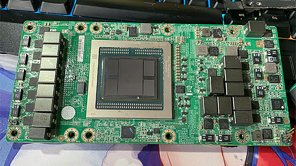
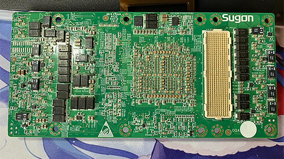
Ultimately we ended up with two systems to test – one commercial ‘Hygon Dhyana’ and one enterprise ‘Hygon Dhyana Plus’.
Para além da óbvia diferença a nível dos algoritmos de criptografia usados no CPU, também há diferença a nível do número de instruções (dependendo das instruções) por cada ciclo, o que não deixa de ser surpreendente...By and large, as we could determine, the core layout is identical, with the same cache sizes, TLB sizes, and port allocations – there were no differences at this fundamental level. The CPU still offered 64 KB 4-way for the L1 instruction cache, 32 KB 8-way for the L1 data cache, 512 KB 8-way for the L2 cache, and 8 MB 16-way for the L3 cache, identical to the Zen 1 core.
Cryptography Changes
For the cryptography changes, these are detailed in the Linux kernel updates. The updates revolve around AMD’s secure encryption for virtualization features, or SEV. Normally with an EPYC processor, SEV is governed by the cryptography protocols defined by AMD, in this case RSA, ECDSA, ECDH, SHA, and AES. In order to generate the right keys, SEV uses these methods. However, in the Hygon Dhyana designs, SEV is built to use algorithms known as SM2, SM3, and SM4.
Slowing Down Some Instructions
In our testing, we found that while integer performance is similar between Hygon and EPYC, certain floating point instructions, namely DIV and SQRT, are not pipelined in the Hygon CPU. This means throughput and latency is reduced. A lot of simple MMX/SSE instructions have reduced throughput:
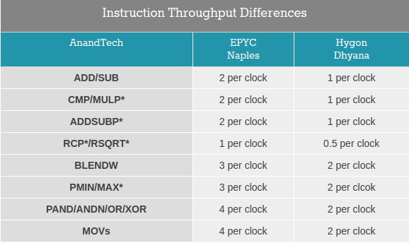
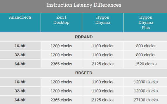
Perhaps the biggest change however was one that even differed between the server ‘Dhyana Plus’ processor and the consumer ‘Dhyana’ version. Random number generation, which is a key backbone in a lot of stochastic and financial processes, is severely reduced on the Dhyana Plus. The key instructions, RDRAND and RDSEED, have various reasons for being slow/fast. Here’s the comparison:
https://www.anandtech.com/show/15493/hygon-dhyana-reviewed-chinese-x86-cpus-amd